Oski Technology

We will be available to chat with you anytime during the conference on our (#s-oskitech )
We will be available online to video chat with you on Monday and Tuesday during breakfast, lunch, and dinner. Please see our (#s-oskitech ) for details.
About Oski
Our mission is to make zero-bug silicon a reality. Oski’s unique exhaustive formal verification solutions deliver peak sign-off confidence earlier in the semiconductor development cycle by diving deep into design behavior to track down the most complex corner-case bugs. Our approach exhaustively proves the absence of bugs and brings a higher level of productivity to our clients, as compared with traditional simulation and formal verification approaches. Since 2005, Oski has focused on developing comprehensive formal verification solutions to identify and sign-off high-risk blocks, achieve system-level architecture sign-off, and quickly resolve post-silicon bugs. Oski has built the largest team of formal verification experts in the world. Our founder, Vigyan Singhal, did his PhD thesis at UC Berkeley in formal methods of verification. Vigyan later developed Cadence’s first-generation formal verification tool, and was the founder of Jasper Design Automation, which was later acquired by Cadence. The company is headquartered in San Jose, CA with a design center in Gurugram, India.
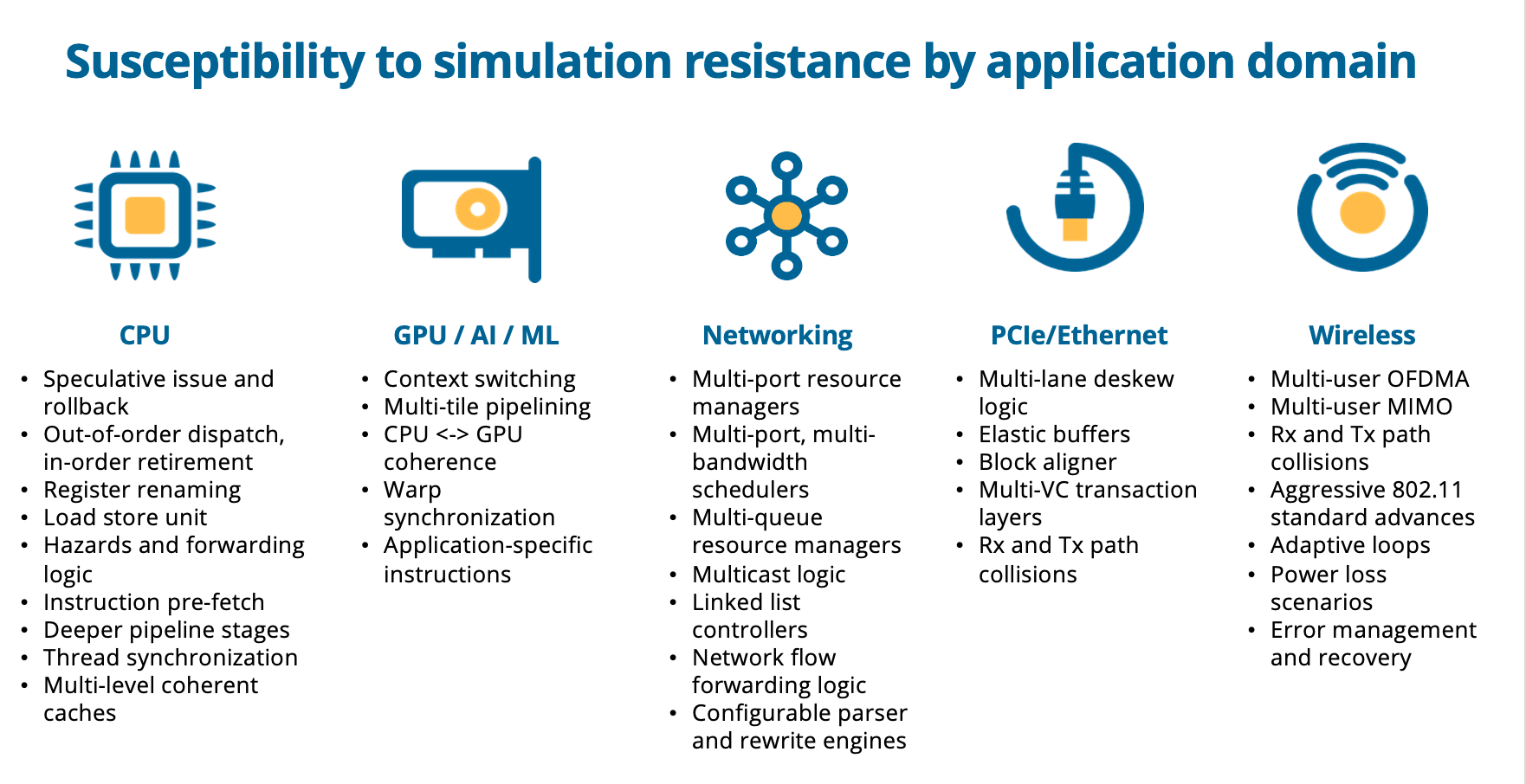
Problem: Parallelism & “Superbugs”
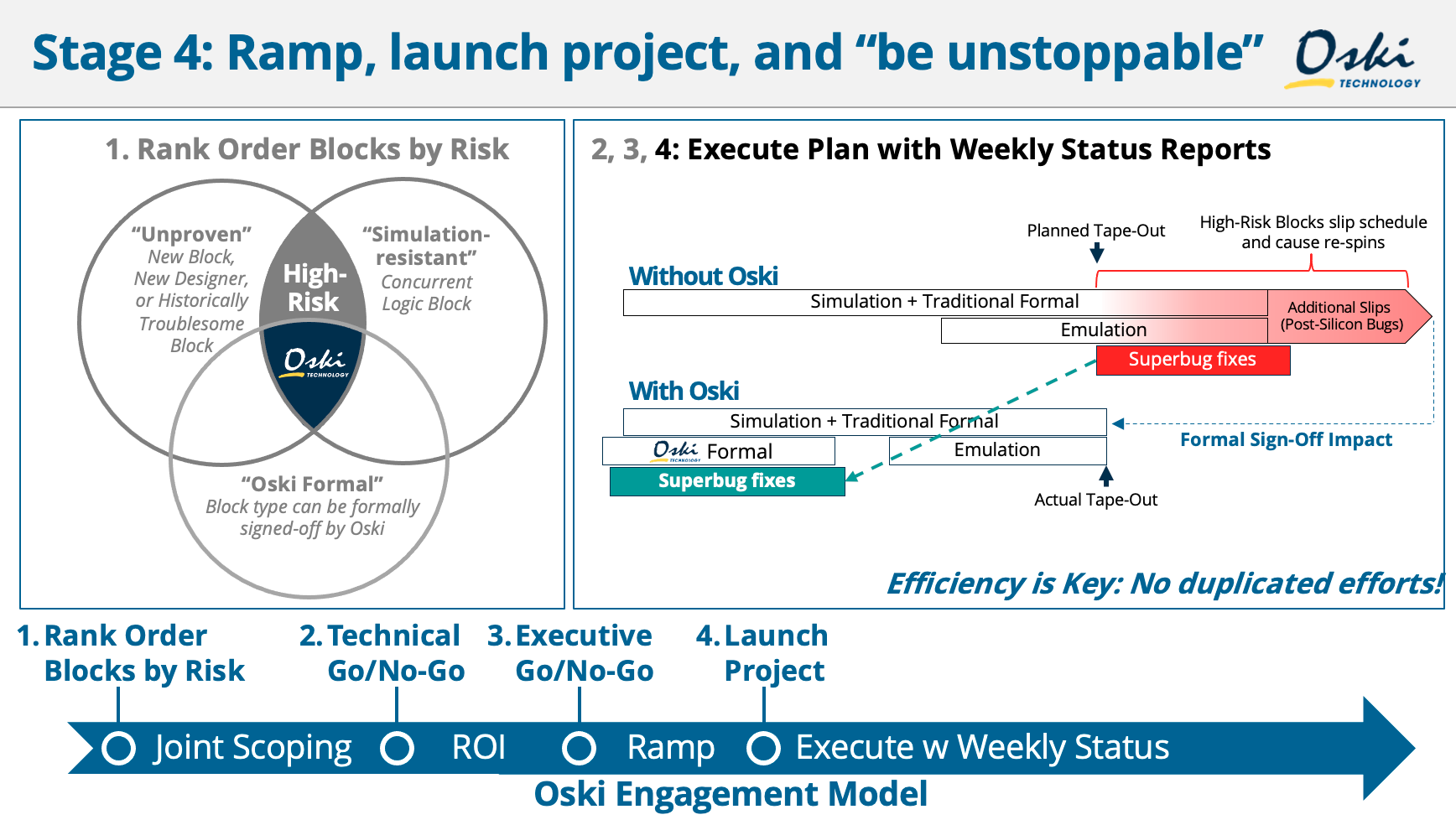
The surge in parallelism and functional complexity has led to an increase in insidious bugs that are impossible to find pre-silicon using simulation or traditional formal methods. High-risk blocks with parallel structures, multiple power modes, concurrent processing, and/or multiple operational modes overwhelm simulation and lead to silicon bug escapes.
These blocks have too many combinations to test in simulation to completely cover all temporal relations between events. Additionally, finding one of these “superbugs” is a strong indicator that there are related bugs nearby, making it difficult to predict when all the bugs will be fixed, and the chip will be approved for tape-out.
Superbugs are always root-caused to concurrent logic blocks and never to sequential logic blocks. To restore chip-level, sign-off confidence we need a verification strategy that will predictably close all logic in “project time”:
-
Concurrent Logic: formal sign-off methods find all bugs, including bugs caused by parallelism, in these high-risk blocks.
-
Sequential Logic: advanced simulation methods can effectively close these blocks.
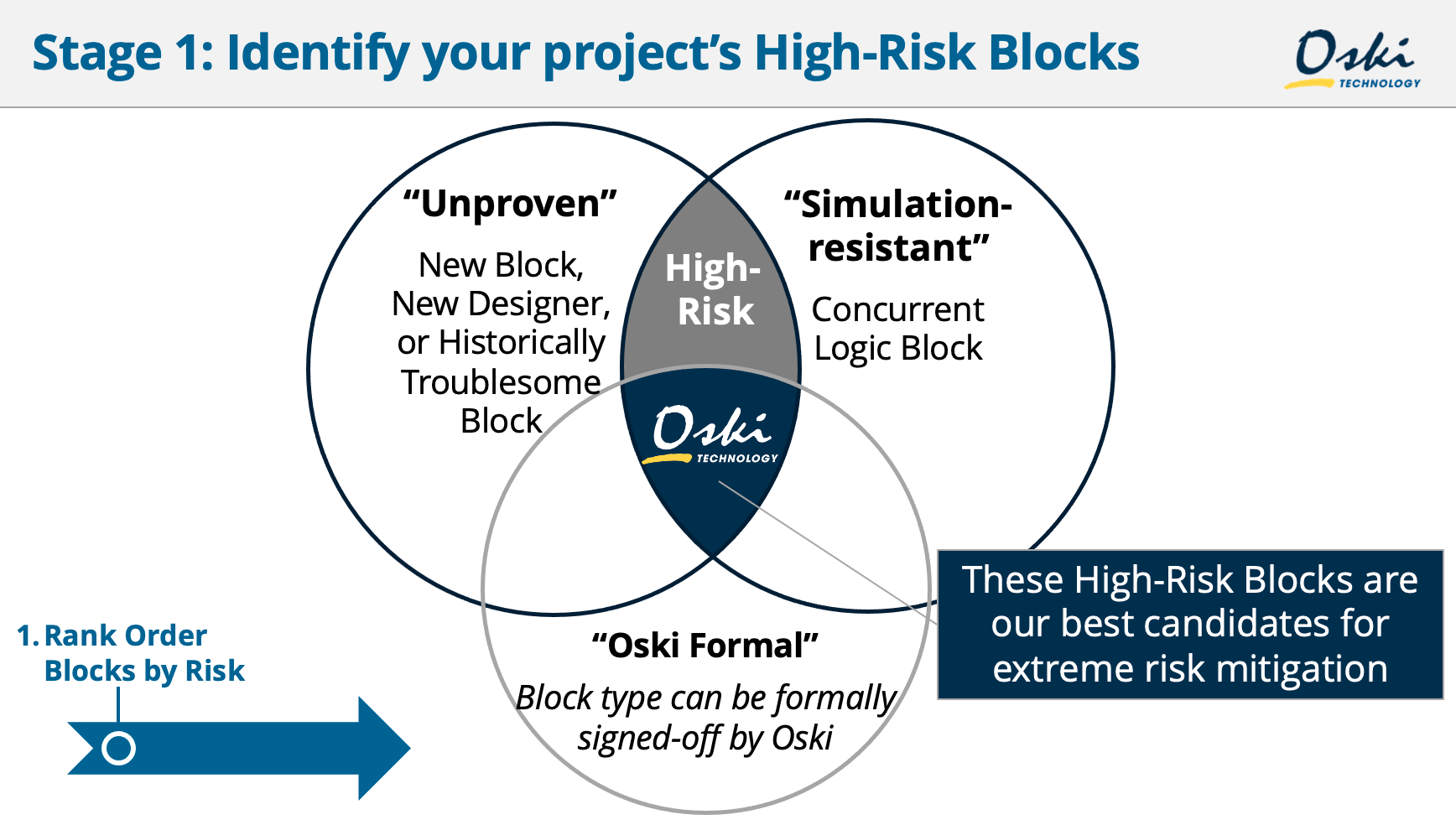
Oski’s High-Risk Block Formal Sign-off is Exhaustive
Formal sign-off proves the absence of bugs. It is the only method that guarantees that all bugs have been found in your high-risk blocks before your schedule says it is time to tape-out.
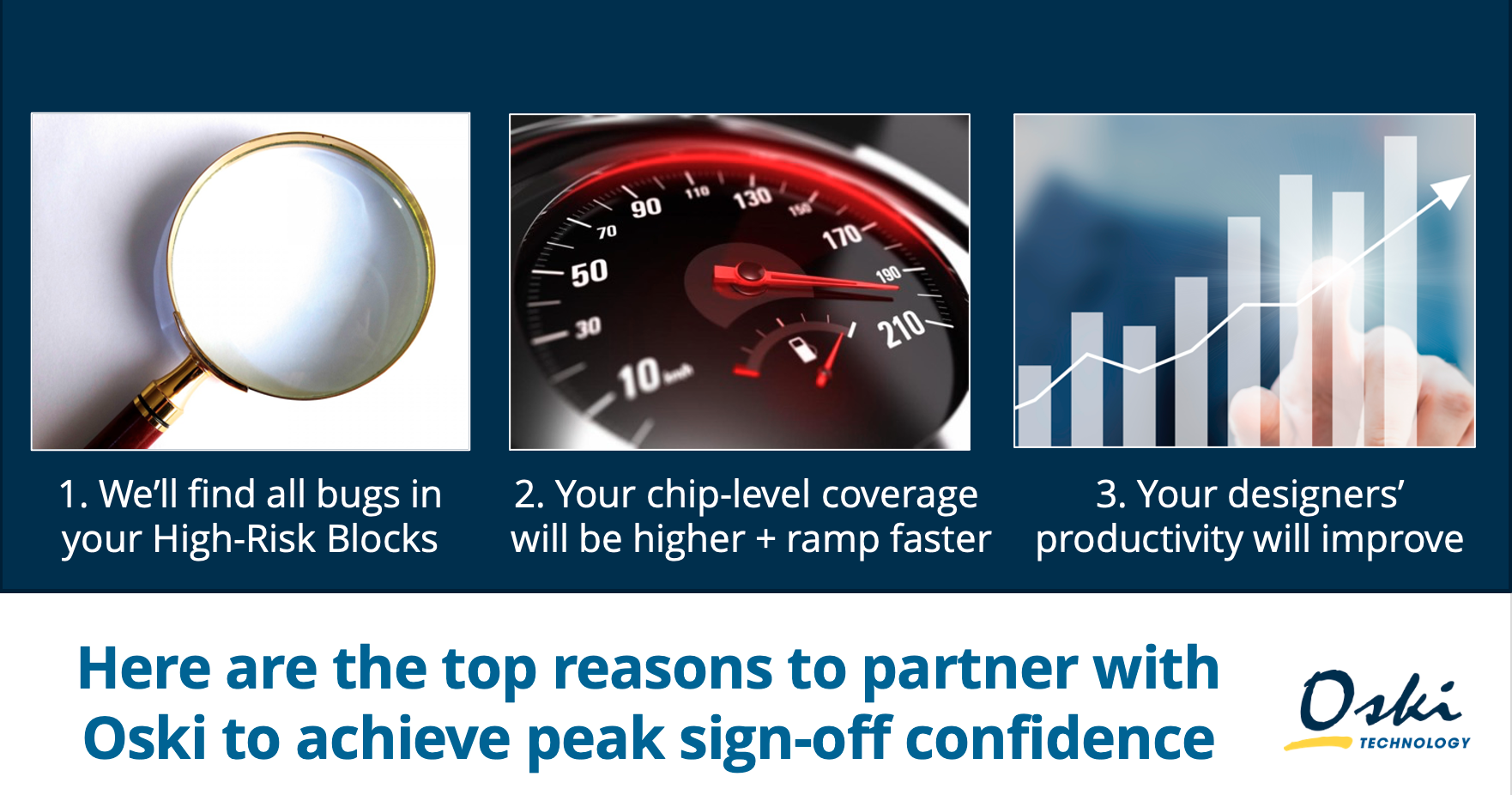
We’ll find all the bugs in your high-risk blocks.
-
We rank your high-risk blocks by bug-escape risk.
-
You will not need to simulate the blocks that we formally sign-off.
-
If you modify your RTL, our follow-on proofs are also exhaustive.
Your chip-level coverage will be higher and ramp faster.
You will know there are no bugs remaining in your High-Risk Blocks.
-
If we start early, we can sign-off your high-risk blocks to be bug-free by mid-project.
-
Formally signing-off the concurrent logic blocks enables your verification team to focus on sequential logic blocks.
Your designers will spend less time on debug.
-
We find major bugs early, so your designers have the freedom to create a proper fix or even re-architect the design.
-
Fewer than 10% of bugs we report are false negatives.
-
It typically takes 5 to 30 minutes to root cause a bug with our concise counterexamples and analysis.
Sign-Off with Confidence
Our Formal Sign-Off Engagement Process is designed to deliver peak, chip-level, tape-out confidence by finding all bugs in your high-risk blocks and confirming that the last bug has been found.
This three-meeting series quickly identifies blocks that are impossible to verify using simulation and traditional formal methods, and builds a Formal Sign-Off Plan for these blocks that replaces block-level simulation. These meetings can be held in-person or via WebEx and are most efficient when you share your project block diagram and verification plan.
Step 1: Discovery Meeting
Goal: Identify a mission-critical project to investigate high-risk blocks. This 60-minute meeting has three elements.
Information Gathering: We ask questions about your current and historical verification challenges, to better understand your exposure to simulation-resistant superbug escapes to silicon.
Oski Presentation: We provide an introductory presentation to explain how our formal sign-off methodologies deliver chip-level impact for your specific project and verification methodologies.
Initial Assessment: If we see potential for our formal sign-off solutions to deliver significant chip-level impact, we will recommend moving forward to the Project Scoping step.
Step 2: Project Scoping
Goal: Rank order high-risk blocks on your mission-critical project by post-silicon bug escape risk.
In this 60 to 90-minute meeting with our RnD team, we dive deeper into your high-risk blocks and rank them by bug escape risk, i.e., simulation resistance.
Following our meeting, Oski’s RnD team will estimate the effort required to formally sign-off your high-risk blocks.
Step 3: Statement of Work Review & Approval
Goal: Jointly review and finalize a formal sign-off Statement of Work (SOW).
In this 60-minute meeting, Oski will present our RnD team’s recommendations for formal sign-off of your high-risk blocks along with a timetable.
Because our team will find all bugs using exhaustive formal sign-off methods, you will not need to simulate these blocks.